The amplifier, the assembly of which we will describe today, despite its relative simplicity, provides fairly high parameters. Of course, “microcircuit” devices have a number of limitations, so “loose” amplifiers can provide higher performance. At the same time, the scheme we have chosen has a number of advantages:
- it is quite simple;
- costs less;
- practically does not require adjustment;
- assembles quickly (literally in the evening);
- The quality is superior to many amplifiers of the 70s and 80s, and it is quite sufficient for most applications (and even modern systems under $300 can be inferior to it);
- This version of the amplifier is universal (suitable for both beginners and experienced radio amateurs).
- See the characteristics - what devices can be created based on it
Basic parameters of the Hi-Fi amplifier on the TDA7294 chip
Let us immediately note that the microcircuit worked stably with an active load of 2–24 Ohms, with an active resistance of 4 Ohms, with a capacitive load of +/- 15 μF, as well as with an inductive load of +/- 1.5 mH. Moreover, the distortion remained small on capacitive and inductive loads. It is worth saying that the amount of distortion strongly depends on the power source (especially with a capacitive load).
You can see the measurement results directly in the table below:
| Parameter | Meaning | Measurement conditions |
| Rout.max, W (long-term sinusoidal) | 36 | Supply voltage +- 22V, Rн = 4 Ohm |
| Frequency range at -3 dB level | 9 Hz–50 kHz | Rн = 8 Ohm, Uout = 4 V |
| Kg, % (using RMAA 5.5 program) | 0,008 | Rн = 8 Ohm, Рout = 16 W, f = 1 kHz |
| Sensitivity, V | 0,5 | Rout.max = 50 W, Rn = 4 Ohm, Uip = +/-27 V |
Hi-Fi amplifier on the TDA7294 chip: circuit diagram and description
Detailed circuit diagram of a Hi-Fi amplifier based on the TDA7294 chip
The circuit of this amplifier is practically a repetition of the switching circuit offered by the manufacturer. And this is no coincidence - who knows better how to turn it on. And there certainly won’t be any surprises due to non-standard activation or operating mode.
Let’s note right away that you won’t get any 80 watts (let alone 100 watts) from it. Realistically 40–60, but these will be honest long-term watts. In a short-term impulse you can get much more, but this will already be RMPO power, by the way, also honest (80–120 W). In “Chinese” watts this will be several thousand. If anyone is interested - five thousand. It all depends heavily on the power source.
And do not forget that a stereo amplifier requires a power supply that is twice as powerful (when calculating using the proposed program, everything is taken into account automatically).
Important!!! There must be a fuse at least in the primary winding of the transformer! Remember that high voltage is dangerous to life, and a short circuit can cause a fire! And one more thing: a fuse cannot be connected to the “ground” circuit!
The circuit also works from a pulsed source, but here high demands are placed on the source itself: small ripples, the ability to deliver current up to 10 amperes without problems, strong “sags” and generation failures. Remember that high-frequency pulsations are suppressed by the microcircuit much worse, so the level of distortion can increase by 10–100 times, although “outwardly” everything is in order. A good switching source suitable for Hi-Fi audio is a complex and expensive device, so making an “old-fashioned” analogue power supply will often be easier and cheaper.
Printed circuit board and amplifier assembly on the TDA7294 chip
The printed circuit board is single-sided and has dimensions of 65x70 mm:


The board is wired taking into account all the requirements for wiring high-quality amplifiers. The entrance is separated as far as possible from the exit, and is enclosed in a “screen” of divided earth - entrance and exit. The power paths ensure maximum efficiency of filter capacitors (in this case, the length of the leads of capacitors C10 and C12 should be minimal). In this experimental board we installed terminal blocks for connecting input, output and power. There is a place for them (the C10 capacitor may be somewhat in the way), but for stationary structures it is better to solder all these wires, because it is more reliable.
In addition to low resistance, wide tracks also have the advantage that they are more difficult to peel off when overheated. And when manufacturing using the “laser-ironing” method, if a 1x1 mm square is not “printed” somewhere, then it’s not a big deal. All the same, the conductor will not break. In addition, a wide conductor holds heavy parts better (while a thin conductor can simply peel off from the board).
There is only one jumper on the board. It lies under the pins of the microcircuit, so it needs to be mounted first, and leave enough space under the pins so that it doesn’t short out.
The following important components were used during installation:
- 0.12 W resistors (except R9);
- capacitors C9, C10, C12 K73-17 63V;
- capacitors C4 K10-47v 6.8 µF 25V.
Any modern electrolytes will do. The board shows the connection polarity of all electrolytic capacitors and the diode. Diode - any low-power rectifier that can withstand a reverse voltage of at least 50 Volts (for example 1N4001-1N4007). It is better not to use high-frequency diodes.
There is room in the corners of the board for holes for M3 mounting screws. You can attach the board only to the chip body, but it is still safer to secure it with screws.
The microcircuit must be installed on a radiator with an area of at least 350 cm2. More is better. In principle, it has thermal protection built into it, but it’s better not to tempt fate. Even if active cooling is assumed, the radiator must still be quite massive: with pulsed heat release, which is typical for music, heat is more effectively removed by the heat capacity of the radiator (that is, a large cold piece of iron) rather than by dissipation into the environment.
The metal housing of the microcircuit is connected to the negative side of the power supply. This gives rise to two ways to install it on a radiator:
- Through an insulating gasket. In this case, the radiator can be electrically connected to the housing.
- Directly, in this case the radiator is necessarily electrically isolated from the body.
The second option provides better cooling, but requires caution (for example, you cannot remove the chip while the power is on).
In both cases, you need to use heat-conducting paste, and in the 1st option it should be applied both between the chip body and the gasket, and between the gasket and the radiator.
You will find a printed circuit board in Sprint-Layout 4.0 format, a diagram in pdf format and the location of parts on the board in gif format in the archive below:
Debugging a Hi-Fi amplifier on the TDA7294 chip
As practice shows, 90% of all problems with equipment are due to its “lack of adjustment.” That is, having soldered yet another circuit and having failed to fix it, the radio amateur gives up on it and publicly declares the circuit bad. Therefore, setup is the most important (and often the most difficult) stage in creating an electronic device.
A properly assembled amplifier does not need adjustment. But, since no one guarantees that all parts are absolutely in good working order, you need to be careful when you turn it on for the first time.
The first switch-on is carried out without load and with the input signal source turned off (it is better to short-circuit the input with a jumper). It would be nice to include fuses of about 1A in the power circuit (both in the “plus” and “minus” between the power source and the amplifier itself). Briefly (about 0.5 sec.) Apply the supply voltage and make sure that the current consumed from the source is small (the fuses do not burn out). It is convenient if the source has LED indicators. When disconnected from the network, the LEDs continue to light for at least 20 seconds: the filter capacitors are discharged for a long time by the small quiescent current of the microcircuit.
If the current consumed by the microcircuit is large (more than 300 mA), then there can be many reasons:
- Short circuit in installation;
- poor contact in the “ground” wire from the source;
- “plus” and “minus” are confused;
- the pins of the microcircuit touch the jumper;
- microcircuit is faulty;
- capacitors C11, C13 are soldered incorrectly;
- capacitors C10-C13 are faulty.
The presence of alternating voltage at the output indicates problems with the microcircuit or circuits C7R9, C3R3R4, R10. Unfortunately, conventional testers often cannot measure the high-frequency voltage that appears during self-excitation (up to 100 kHz), so it is best to use an oscilloscope here.
If everything is in order here, we connect the load, check again for the absence of excitation with the load and that’s it - you can listen!
But it’s better to do another test. The fact is that the most disgusting type of amplifier excitation is “ringing” (when excitation appears only in the presence of a signal, and at a certain amplitude). The main problem is that it is difficult to detect without an oscilloscope and an audio generator (and it is not easy to eliminate), and the sound deteriorates enormously due to huge intermodulation distortion. By ear, this is usually perceived as a “heavy” sound, that is, without any additional overtones (since the frequency is very high), so the listener does not know that his amplifier is being excited. He just listens and decides that the microcircuit is “bad” and “doesn’t sound.” With proper assembly of the amplifier and a normal power source, this should not happen.

Graphic representation of amplifier "ringing"
However, sometimes such distortions occur, and the C7R9 circuit is precisely what fights them. But in a normal microcircuit everything is fine even in the absence of C7R9. We came across examples of microcircuits with a ringing sound. In them, the problem was solved by introducing the C7R9 circuit (that’s why we use it, even though it’s not in the datasheet). If such a nasty thing occurs even if you have a C7R9, then you can try to eliminate it by “playing” with the resistance (it can be reduced to 3 ohms), but we would not recommend using such a microcircuit. This is definitely some kind of marriage, and who knows what else will come out of it.
As we noted above, “ringing” can only be seen on an oscilloscope, and not all radio amateurs have this equipment. Although, if you want to get good at radio electronics, try to get hold of such devices or at least use them somewhere. To always get high-quality sound, you must definitely check it on the devices. Remember, “ringing” is a most insidious thing that can ruin the sound in a thousand ways.
You can view another method of assembling a Hi-Fi amplifier on the TDA7294 chip in the video below:
Introduction
The subwoofer amplifier was made not due to lack of or saving money, but for the sake of interest. At the same time, my son did the same with me (he had already done 2 pieces).
I am not a music lover or an audiophile, but I love music and listen to it often. I’m not deprived of hearing, but at the same time, I don’t understand people who start reading hundredths of nonlinear distortions, talking about the direction of wires and the audibility of high frequencies in the almost ultrasonic range. All this is bullshit and is called the word “disease”. Not all people are endowed with perfect hearing, so everyone has their own ceiling. The main thing in music is that it gives pleasure. If you like the sound of your radio, acoustics, amplifier, then here's happiness for you. Now all that remains is to make an amplifier and a power supply for it (voltage converter).
Subwoofer amplifier based on TDA7294 (bridge circuit)
 Why TDA7294? Very cheap for beginners, good parameters. The amplifier is very simple to manufacture. There are plenty of printed circuit boards on the Internet. I made my own signet to match my body. Notget hung up on finding the perfect board. Take the one that suits you in design and size. Almost any board that does not contain errors will work. It is desirable that the ground converge at one point, but if this is not the case, then it is not a fact that the circuit will not work or be excited. On my board, pins 1 and 4 of the microcircuit do not go to ground individually, but are connected in series. Everything works without problems. If this is your first time assembling such circuits, then it is best to assemble a standard switching circuit. All schemes like Syritso and other homemade products may not work, since they were customized by the authors to suit themselves and their details. The typical switching circuit is not critical to the parts used and, if installed correctly, starts working immediately. Power supply capacitors are not necessarily of large capacity. 2200 uF for the ears. The big disadvantage of the circuit is the heat dissipation, so the radiator is larger. I used what was at hand (it turned out to be too small), it gets very hot, I had to install three 50x50 mm fans (now the radiator is slightly warm). If possible, it is better to install a large radiator without relying on fans, as the fans may fail. They don’t work in computers for long, but in the trunk they will even die ahead of time. Another truism is that microcircuits are placed on the radiator only through insulating gaskets and preferably thermal paste.
My PCB is 100% working. Made using ironing technology. If anyone repeats it, then solder the power supply tracks and the speaker output.

 A few words about the crossover. Scheme from Shikhatov’s website. The scheme requires no explanation. The 544UD2 microcircuit and its foreign analog did not work for me (I changed several microcircuits). Excited at a frequency of about 1 MHz. I changed it to UD6 and everything became normal. Use good variables, otherwise there will be cod in the dynamics.


Each case has its own design; I made it using old proven technology from foil-coated PCB. It is inexpensive, well processed, the body is strong and beautiful. Painted with anti-gravel. The power connector and speaker were homemade, using part of a powerful relay. The amplifier is a complete structure. At 35 volts it produces 180 W of undistorted signal (according to the oscilloscope).


PS: For me the amp was cheap, but if you don't have parts in stock and have to buy everything, it will represent a certain amount of money. First, calculate the costs, and then get to work. In any case, this amplifier is ideal for entry-level.

A low frequency amplifier (LFA) is a device for amplifying electrical oscillations corresponding to the frequency range audible to the human ear, i.e. the LFA should amplify in the frequency range from 20 Hz to 20 kHz, but some VLFs can have a range of up to 200 kHz. The ULF can be assembled as an independent device, or used in more complex devices - televisions, radios, radios, etc.
The peculiarity of this circuit is that pin 11 of the TDA1552 microcircuit controls the operating modes - Normal or MUTE.

C1, C2 - pass-through blocking capacitors, used to cut off the constant component of the sinusoidal signal. It is better not to use electrolytic capacitors. It is advisable to place the TDA1552 chip on a radiator using heat-conducting paste.
In principle, the presented circuits are bridge ones, because in one housing of the TDA1558Q microassembly there are 4 amplification channels, so pins 1 - 2, and 16 - 17 are connected in pairs, and they receive input signals from both channels through capacitors C1 and C2. But if you need an amplifier for four speakers, then you can use the circuit option below, although the power will be 2 times less per channel.
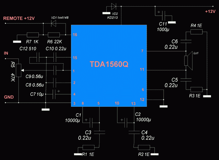
The basis of the design is the TDA1560Q class H microassembly. The maximum power of this ULF reaches 40 W, with a load of 8 ohms. This power is provided by approximately twice the increased voltage due to the operation of the capacitors.
The output power of the amplifier in the first circuit assembled on the TDA2030 is 60W at a load of 4 Ohms and 80W at a load of 2 Ohms; TDA2030A 80W at 4 ohm load and 120W at 2 ohm load. The second circuit of the considered ULF is already with an output power of 14 Watts.

This is a typical two-channel ULF. With a little wiring of passive radio components, this chip can be used to build an excellent stereo amplifier with an output power of 1 W on each channel.
The TDA7265 microassembly is a fairly powerful two-channel Hi-Fi class AB amplifier in a standard Multiwatt package; the microcircuit has found its niche in high-quality stereo technology, Hi-Fi class. The simple switching circuit and excellent parameters made the TDA7265 a perfectly balanced and excellent solution for building high-quality amateur radio equipment.
First, a test version was assembled on a breadboard exactly as shown in the datasheet in the link above, and successfully tested on S90 speakers. The sound is not bad, but something was missing. After some time, I decided to remake the amplifier using a modified circuit.
The microassembly is a quad class AB amplifier designed specifically for use in car audio devices. Based on this microcircuit, you can build several high-quality ULF options using a minimum of radio components. The microcircuit can be recommended to beginning radio amateurs for home assembly of various speaker systems.
The main advantage of the amplifier circuit on this microassembly is the presence of four channels independent of each other. This power amplifier operates in AB mode. It can be used to amplify various stereo signals. If desired, you can connect it to the speaker system of a car or personal computer.
The TDA8560Q is just a more powerful analogue of the TDA1557Q chip, widely known to radio amateurs. The developers have only strengthened the output stage, making the ULF perfectly suited to a two-ohm load.
The LM386 microassembly is a ready-made power amplifier that can be used in designs with low supply voltage. For example, when powering the circuit from a battery. LM386 has a voltage gain of about 20. But by connecting external resistances and capacitances, the gain can be adjusted up to 200, and the output voltage automatically becomes equal to half the supply voltage.
The LM3886 microassembly is a high quality amplifier with an output power of 68 watts into a 4 ohm load or 50 watts into 8 ohms. At peak moment, the output power can reach 135 W. A wide voltage range from 20 to 94 volts is applicable to the microcircuit. Moreover, you can use both bipolar and unipolar power supplies. The ULF harmonic coefficient is 0.03%. Moreover, this is over the entire frequency range from 20 to 20,000 Hz.

The circuit uses two ICs in a typical connection - KR548UH1 as a microphone amplifier (installed in the PTT switch) and (TDA2005) in a bridge connection as a final amplifier (installed in the siren housing instead of the original board). A modified alarm siren with a magnetic head is used as an acoustic emitter (piezo emitters are not suitable). The modification consists of disassembling the siren and throwing out the original tweeter with an amplifier. The microphone is electrodynamic. When using an electret microphone (for example, from Chinese handsets), the connection point between the microphone and the capacitor must be connected via a ~4.7K resistor to +12V (after the button!). The 100K resistor in the K548UH1 feedback circuit is better set with a resistance of ~30-47K. This resistor is used to adjust the volume. It is better to install the TDA2004 chip on a small radiator.
Test and operate - with the emitter under the hood and the PTT in the cabin. Otherwise, squealing due to self-excitation is inevitable. A trimmer resistor sets the volume level so that there is no strong sound distortion and self-excitation. If the volume is insufficient (for example, a bad microphone) and there is a clear reserve of emitter power, you can increase the gain of the microphone amplifier by several times increasing the value of the trimmer in the feedback circuit (the one according to the 100K circuit). In a good way, we would also need a primabass that would prevent the circuit from self-exciting - some kind of phase-shifting chain or a filter for the excitation frequency. Although the scheme works fine without complications
Currently, a wide range of imported integrated low-frequency amplifiers has become available. Their advantages are satisfactory electrical parameters, the ability to select microcircuits with a given output power and supply voltage, stereophonic or quadraphonic design with the possibility of bridge connection.
To manufacture a structure based on an integral ULF, a minimum of attached parts is required. The use of known-good components ensures high repeatability and, as a rule, no additional tuning is required.
The given typical switching circuits and main parameters of integrated ULFs are designed to facilitate the orientation and selection of the most suitable microcircuit.
For quadraphonic ULFs, the parameters in bridged stereo are not specified.
TDA1010
Supply voltage - 6...24 V
Output power (Un =14.4 V, THD = 10%):
RL=2 Ohm - 6.4 W
RL=4 Ohm - 6.2 W
RL=8 Ohm - 3.4 W
Quiescent current - 31 mA
Connection diagram
TDA1011
Supply voltage - 5.4...20 V
Maximum current consumption - 3 A
Un=16V - 6.5 W
Un=12V - 4.2 W
Un=9V - 2.3 W
Un=6B - 1.0 W
SOI (P=1 W, RL=4 Ohm) - 0.2%
Quiescent current - 14 mA
Connection diagram
TDA1013
Supply voltage - 10...40 V
Output power (THD=10%) - 4.2 W
THD (P=2.5 W, RL=8 Ohm) - 0.15%
Connection diagram
TDA1015
Supply voltage - 3.6...18 V
Output power (RL=4 Ohm, THD=10%):
Un=12V - 4.2 W
Un=9V - 2.3 W
Un=6B - 1.0 W
SOI (P=1 W, RL=4 Ohm) - 0.3%
Quiescent current - 14 mA
Connection diagram
TDA1020
Supply voltage - 6...18 V
RL=2 Ohm - 12 W
RL=4 Ohm - 7 W
RL=8 Ohm - 3.5 W
Quiescent current - 30 mA
Connection diagram
TDA1510
Supply voltage - 6...18 V
Maximum current consumption - 4 A
THD=0.5% - 5.5 W
THD=10% - 7.0 W
Quiescent current - 120 mA
Connection diagram
TDA1514
Supply voltage - ±10...±30 V
Maximum current consumption - 6.4 A
Output power:
Un =±27.5 V, R=8 Ohm - 40 W
Un =±23 V, R=4 Ohm - 48 W
Quiescent current - 56 mA
Connection diagram
TDA1515
Supply voltage - 6...18 V
Maximum current consumption - 4 A
RL=2 Ohm - 9 W
RL=4 Ohm - 5.5 W
RL=2 Ohm - 12 W
RL4 Ohm - 7 W
Quiescent current - 75 mA
Connection diagram
TDA1516
Supply voltage - 6...18 V
Maximum current consumption - 4 A
Output power (Un =14.4 V, THD = 0.5%):
RL=2 Ohm - 7.5 W
RL=4 Ohm - 5 W
Output power (Un =14.4 V, THD = 10%):
RL=2 Ohm - 11 W
RL=4 Ohm - 6 W
Quiescent current - 30 mA
Connection diagram
TDA1517
Supply voltage - 6...18 V
Maximum current consumption - 2.5 A
Output power (Un=14.4B RL=4 Ohm):
THD=0.5% - 5 W
THD=10% - 6 W
Quiescent current - 80 mA
Connection diagram
TDA1518
Supply voltage - 6...18 V
Maximum current consumption - 4 A
Output power (Un =14.4 V, THD = 0.5%):
RL=2 Ohm - 8.5 W
RL=4 Ohm - 5 W
Output power (Un =14.4 V, THD = 10%):
RL=2 Ohm - 11 W
RL=4 Ohm - 6 W
Quiescent current - 30 mA
Connection diagram
TDA1519
Supply voltage - 6...17.5 V
Maximum current consumption - 4 A
Output power (Up=14.4 V, THD=0.5%):
RL=2 Ohm - 6 W
RL=4 Ohm - 5 W
Output power (Un =14.4 V, THD = 10%):
RL=2 Ohm - 11 W
RL=4 Ohm - 8.5 W
Quiescent current - 80 mA
Connection diagram
TDA1551
Supply voltage -6...18 V
THD=0.5% - 5 W
THD=10% - 6 W
Quiescent current - 160 mA
Connection diagram
TDA1521
Supply voltage - ±7.5...±21 V
Output power (Un=±12 V, RL=8 Ohm):
THD=0.5% - 6 W
THD=10% - 8 W
Quiescent current - 70 mA
Connection diagram
TDA1552
Supply voltage - 6...18 V
Maximum current consumption - 4 A
Output power (Un =14.4 V, RL = 4 Ohm):
THD=0.5% - 17 W
THD=10% - 22 W
Quiescent current - 160 mA
Connection diagram
TDA1553
Supply voltage - 6...18 V
Maximum current consumption - 4 A
Output power (Up=4.4 V, RL=4 Ohm):
THD=0.5% - 17 W
THD=10% - 22 W
Quiescent current - 160 mA
Connection diagram
TDA1554
Supply voltage - 6...18 V
Maximum current consumption - 4 A
THD=0.5% - 5 W
THD=10% - 6 W
Quiescent current - 160 mA
Connection diagram
TDA2004
Output power (Un=14.4 V, THD=10%):
RL=4 Ohm - 6.5 W
RL=3.2 Ohm - 8.0 W
RL=2 Ohm - 10 W
RL=1.6 Ohm - 11 W
KHI (Un=14.4V, P=4.0 W, RL=4 Ohm) - 0.2%;
Bandwidth (at -3 dB level) - 35...15000 Hz
Quiescent current -<120 мА
Connection diagram
TDA2005
Dual integrated ULF, designed specifically for use in cars and allowing operation with low-impedance loads (up to 1.6 Ohms).
Supply voltage - 8...18 V
Maximum current consumption - 3.5 A
Output power (Up = 14.4 V, THD = 10%):
RL=4 Ohm - 20 W
RL=3.2 Ohm - 22 W
SOI (Uп =14.4 V, Р=15 W, RL=4 Ohm) - 10%
Bandwidth (level -3 dB) - 40...20000 Hz
Quiescent current -<160 мА
Connection diagram
TDA2006
The pin layout matches the pin layout of the TDA2030 chip.
Supply voltage - ±6.0...±15 V
Maximum current consumption - 3 A
Output power (Ep=±12V, THD=10%):
at RL=4 Ohm - 12 W
at RL=8 Ohm - 6...8 W THD (Ep=±12V):
at P=8 W, RL= 4 Ohm - 0.2%
at P=4 W, RL= 8 Ohm - 0.1%
Bandwidth (at -3 dB level) - 20...100000 Hz
Consumption current:
at P=12 W, RL=4 Ohm - 850 mA
at P=8 W, RL=8 Ohm - 500 mA
Connection diagram
TDA2007
Dual integrated ULF with single-row pin arrangement, specially designed for use in television and portable radio receivers.
Supply voltage - +6...+26 V
Quiescent current (Ep=+18 V) - 50...90 mA
Output power (THD=0.5%):
at Ep=+18 V, RL=4 Ohm - 6 W
at Ep=+22 V, RL=8 Ohm - 8 W
SOI:
at Ep=+18 V P=3 W, RL=4 Ohm - 0.1%
at Ep=+22 V, P=3 W, RL=8 Ohm - 0.05%
Bandwidth (at -3 dB level) - 40...80000 Hz
Connection diagram
TDA2008
Integrated ULF, designed to operate on low-impedance loads, providing high output current, very low harmonic content and intermodulation distortion.
Supply voltage - +10...+28 V
Quiescent current (Ep=+18 V) - 65...115 mA
Output power (Ep=+18V, THD=10%):
at RL=4 Ohm - 10...12 W
at RL=8 Ohm - 8 W
SOI (Ep= +18 V):
at P=6 W, RL=4 Ohm - 1%
at P=4 W, RL=8 Ohm - 1%
Maximum current consumption - 3 A
Connection diagram
TDA2009
Dual integrated ULF, designed for use in high-quality music centers.
Supply voltage - +8...+28 V
Quiescent current (Ep=+18 V) - 60...120 mA
Output power (Ep=+24 V, THD=1%):
at RL=4 Ohm - 12.5 W
at RL=8 Ohm - 7 W
Output power (Ep=+18 V, THD=1%):
at RL=4 Ohm - 7 W
at RL=8 Ohm - 4 W
SOI:
at Ep= +24 V, P=7 W, RL=4 Ohm - 0.2%
at Ep= +24 V, P=3.5 W, RL=8 Ohm - 0.1%
at Ep= +18 V, P=5 W, RL=4 Ohm - 0.2%
at Ep= +18 V, P=2.5 W, RL=8 Ohm - 0.1%
Maximum current consumption - 3.5 A
Connection diagram
TDA2030
Integrated ULF, providing high output current, low harmonic content and intermodulation distortion.
Supply voltage - ±6...±18 V
Quiescent current (Ep=±14 V) - 40...60 mA
Output power (Ep=±14 V, THD = 0.5%):
at RL=4 Ohm - 12...14 W
at RL=8 Ohm - 8...9 W
SOI (Ep=±12V):
at P=12 W, RL=4 Ohm - 0.5%
at P=8 W, RL=8 Ohm - 0.5%
Bandwidth (at -3 dB level) - 10...140000 Hz
Consumption current:
at P=14 W, RL=4 Ohm - 900 mA
at P=8 W, RL=8 Ohm - 500 mA
Connection diagram
TDA2040
Integrated ULF, providing high output current, low harmonic content and intermodulation distortion.
Supply voltage - ±2.5...±20 V
Quiescent current (Ep=±4.5...±14 V) - mA 30...100 mA
Output power (Ep=±16 V, THD = 0.5%):
at RL=4 Ohm - 20...22 W
at RL=8 Ohm - 12 W
THD (Ep=±12V, P=10 W, RL = 4 Ohm) - 0.08%
Maximum current consumption - 4 A
Connection diagram
TDA2050
Integrated ULF, providing high output power, low harmonic content and intermodulation distortion. Designed to work in Hi-Fi stereo systems and high-end TVs.
Supply voltage - ±4.5...±25 V
Quiescent current (Ep=±4.5...±25 V) - 30...90 mA
Output power (Ep=±18, RL = 4 Ohm, THD = 0.5%) - 24...28 W
SOI (Ep=±18V, P=24Wt, RL=4 Ohm) - 0.03...0.5%
Bandwidth (at -3 dB level) - 20...80000 Hz
Maximum current consumption - 5 A
Connection diagram
TDA2051
Integrated ULF, which has a small number of external elements and provides low harmonic content and intermodulation distortion. The output stage operates in class AB, which allows for greater output power.
Output power:
at Ep=±18 V, RL=4 Ohm, THD=10% - 40 W
at Ep=±22 V, RL=8 Ohm, THD=10% - 33 W
Connection diagram
TDA2052
Integrated ULF, the output stage of which operates in class AB. Accepts a wide range of supply voltages and has a high output current. Designed for use in television and radio receivers.
Supply voltage - ±6...±25 V
Quiescent current (En = ±22 V) - 70 mA
Output power (Ep = ±22 V, THD = 10%):
at RL=8 Ohm - 22 W
at RL=4 Ohm - 40 W
Output power (En = 22 V, THD = 1%):
at RL=8 Ohm - 17 W
at RL=4 Ohm - 32 W
SOI (with a passband at the level of -3 dB 100... 15000 Hz and Pout = 0.1... 20 W):
at RL=4 Ohm -<0,7 %
at RL=8 Ohm -<0,5 %
Connection diagram
TDA2611
Integrated ULF designed for use in household equipment.
Supply voltage - 6...35 V
Quiescent current (Ep=18 V) - 25 mA
Maximum current consumption - 1.5 A
Output power (THD=10%): at Ep=18 V, RL=8 Ohm - 4 W
at Ep=12V, RL=8 0m - 1.7 W
at Ep=8.3 V, RL=8 Ohm - 0.65 W
at Ep=20 V, RL=8 Ohm - 6 W
at Ep=25 V, RL=15 Ohm - 5 W
THD (at Pout=2 W) - 1%
Bandwidth - >15 kHz
Connection diagram
TDA2613
SOI:
(Ep=24 V, RL=8 Ohm, Pout=6 W) - 0.5%
(En=24 V, RL=8 Ohm, Pout=8 W) - 10%
Quiescent current (Ep=24 V) - 35 mA
Connection diagram
TDA2614
Integrated ULF, designed for use in household equipment (television and radio receivers).
Supply voltage - 15...42 V
Maximum current consumption - 2.2 A
Quiescent current (Ep=24 V) - 35 mA
SOI:
(Ep=24 V, RL=8 Ohm, Pout=6.5 W) - 0.5%
(Ep=24 V, RL=8 Ohm, Pout=8.5 W) - 10%
Bandwidth (level -3 dB) - 30...20000 Hz
Connection diagram
TDA2615
Dual ULF, designed for use in stereo radios or televisions.
Supply voltage - ±7.5...21 V
Maximum current consumption - 2.2 A
Quiescent current (Ep=7.5...21 V) - 18...70 mA
Output power (Ep=±12 V, RL=8 Ohm):
THD=0.5% - 6 W
THD=10% - 8 W
Bandwidth (at level -3 dB and Pout = 4 W) - 20...20000 Hz
Connection diagram
TDA2822
Dual ULF, designed for use in portable radios and television receivers.
Quiescent current (Ep=6 V) - 12 mA
Output power (THD=10%, RL=4 Ohm):
Ep=9V - 1.7 W
Ep=6V - 0.65 W
Ep=4.5V - 0.32 W
Connection diagram
TDA7052
ULF designed for use in battery-powered wearable audio devices.
Supply voltage - 3...15V
Maximum current consumption - 1.5A
Quiescent current (E p = 6 V) -<8мА
Output power (Ep = 6 V, R L = 8 Ohm, THD = 10%) - 1.2 W
Connection diagram
TDA7053
Dual ULF, designed for use in wearable audio devices, but can also be used in any other equipment.
Supply voltage - 6...18 V
Maximum current consumption - 1.5 A
Quiescent current (E p = 6 V, R L = 8 Ohm) -<16 mA
Output power (E p = 6 V, RL = 8 Ohm, THD = 10%) - 1.2 W
SOI (E p = 9 V, R L = 8 Ohm, Pout = 0.1 W) - 0.2%
Operating frequency range - 20...20000 Hz
Connection diagram
TDA2824
Dual ULF designed for use in portable radio and television receivers
Supply voltage - 3...15 V
Maximum current consumption - 1.5 A
Quiescent current (Ep=6 V) - 12 mA
Output power (THD=10%, RL=4 Ohm)
Ep=9 V - 1.7 W
Ep=6 V - 0.65 W
Ep=4.5 V - 0.32 W
THD (Ep=9 V, RL=8 Ohm, Pout=0.5 W) - 0.2%
Connection diagram
TDA7231
ULF with a wide range of supply voltages, designed for use in portable radios, cassette recorders, etc.
Supply voltage - 1.8...16 V
Quiescent current (Ep=6 V) - 9 mA
Output power (THD=10%):
En=12B, RL=6 Ohm - 1.8 W
En=9B, RL=4 Ohm - 1.6 W
Ep=6 V, RL=8 Ohm - 0.4 W
Ep=6 V, RL=4 Ohm - 0.7 W
Ep=3 V, RL=4 Ohm - 0.11 W
Ep=3 V, RL=8 Ohm - 0.07 W
THD (Ep=6 V, RL=8 Ohm, Pout=0.2 W) - 0.3%
Connection diagram
TDA7235
ULF with a wide range of supply voltages, designed for use in portable radio and television receivers, cassette recorders, etc.
Supply voltage - 1.8...24 V
Maximum current consumption - 1.0 A
Quiescent current (Ep=12 V) - 10 mA
Output power (THD=10%):
Ep=9 V, RL=4 Ohm - 1.6 W
Ep=12 V, RL=8 Ohm - 1.8 W
Ep=15 V, RL=16 Ohm - 1.8 W
Ep=20 V, RL=32 Ohm - 1.6 W
THD (Ep=12V, RL=8 Ohm, Pout=0.5 W) - 1.0%
Connection diagram
TDA7240
Quiescent current (Ep=14.4 V) - 120 mA
RL=4 Ohm - 20 W
RL=8 Ohm - 12 W
SOI:
(Ep=14.4 V, RL=8 Ohm, Pout=12W) - 0.05%
Connection diagram
TDA7241
Bridged ULF, designed for use in car radios. It has protection against short circuits in the load, as well as overheating.
Maximum supply voltage - 18 V
Maximum current consumption - 4.5 A
Quiescent current (Ep=14.4 V) - 80 mA
Output power (Ep=14.4 V, THD=10%):
RL=2 Ohm - 26 W
RL=4 Ohm - 20 W
RL=8 Ohm - 12 W
SOI:
(Ep=14.4 V, RL=4 Ohm, Pout=12 W) - 0.1%
(Ep=14.4 V, RL=8 Ohm, Pout=6 W) - 0.05%
Bandwidth level -3 dB (RL=4 Ohm, Pout=15 W) - 30...25000 Hz
Connection diagram
TDA1555Q
Supply voltage - 6...18 V
Maximum current consumption - 4 A
Output power (Up = 14.4 V. RL = 4 Ohm):
- THD=0.5% - 5 W
- THD=10% - 6 W Quiescent current - 160 mA
Connection diagram
TDA1557Q
Supply voltage - 6...18 V
Maximum current consumption - 4 A
Output power (Up = 14.4 V, RL = 4 Ohm):
- THD=0.5% - 17 W
- THD=10% - 22 W
Quiescent current, mA 80
Connection diagram
TDA1556Q
Supply voltage -6...18 V
Maximum current consumption -4 A
Output power: (Up=14.4 V, RL=4 Ohm):
- THD=0.5%, - 17 W
- THD=10% - 22 W
Quiescent current - 160 mA
Connection diagram
TDA1558Q
Supply voltage - 6..18 V
Maximum current consumption - 4 A
Output power (Up=14 V, RL=4 Ohm):
- THD=0.6% - 5 W
- THD=10% - 6 W
Quiescent current - 80 mA
Connection diagram
TDA1561
Supply voltage - 6...18 V
Maximum current consumption - 4 A
Output power (Up=14V, RL=4 Ohm):
- THD=0.5% - 18 W
- THD=10% - 23 W
Quiescent current - 150 mA
Connection diagram
TDA1904
Supply voltage - 4...20 V
Maximum current consumption - 2 A
Output power (RL=4 Ohm, THD=10%):
- Up=14 V - 4 W
- Up=12V - 3.1 W
- Up=9 V - 1.8 W
- Up=6 V - 0.7 W
SOI (Up=9 V, P<1,2 Вт, RL=4 Ом) - 0,3 %
Quiescent current - 8...18 mA
Connection diagram
TDA1905
Supply voltage - 4...30 V
Maximum current consumption - 2.5 A
Output power (THD=10%)
- Up=24 V (RL=16 Ohm) - 5.3 W
- Up=18V (RL=8 Ohm) - 5.5 W
- Up=14 V (RL=4 Ohm) - 5.5 W
- Up=9 V (RL=4 Ohm) - 2.5 W
SOI (Up=14 V, P<3,0 Вт, RL=4 Ом) - 0,1 %
Quiescent current -<35 мА
Connection diagram
TDA1910
Supply voltage - 8...30 V
Maximum current consumption - 3 A
Output power (THD=10%):
- Up=24 V (RL=8 Ohm) - 10 W
- Up=24 V (RL=4 Ohm) - 17.5 W
- Up=18 V (RL=4 Ohm) - 9.5 W
SOI (Up=24 V, P<10,0 Вт, RL=4 Ом) - 0,2 %
Quiescent current -<35 мА
Connection diagram
TDA2003
Supply voltage - 8...18 V
Maximum current consumption - 3.5 A
Output power (Up=14V, THD=10%):
- RL=4.0 Ohm - 6 W
- RL=3.2 Ohm - 7.5 W
- RL=2.0 Ohm - 10 W
- RL=1.6 Ohm - 12 W
SOI (Up=14.4 V, P<4,5 Вт, RL=4 Ом) - 0,15 %
Quiescent current -<50 мА
Connection diagram
TDA7056
ULF designed for use in portable radio and television receivers.
Supply voltage - 4.5...16 V Maximum current consumption - 1.5 A
Quiescent current (E p = 12 V, R = 16 Ohm) -<16 мА
Output power (E P = 12 V, R L = 16 Ohm, THD = 10%) - 3.4 W
THD (E P = 12 V, R L = 16 Ohm, Pout = 0.5 W) - 1%
Operating frequency range - 20...20000 Hz
Connection diagram
TDA7245
ULF designed for use in wearable audio devices, but can also be used in any other equipment.Supply voltage - 12...30 V
Maximum current consumption - 3.0 A
Quiescent current (E p = 28 V) -<35 мА
Output power (THD = 1%):
-E p = 14 V, R L = 4 Ohm - 4 W
-E P = 18 V, R L = 8 Ohm - 4 W
Output power (THD = 10%):
-E P = 14 V, R L = 4 Ohm - 5 W
-E P = 18 V, R L = 8 Ohm - 5 W
SOI,%
-E P = 14 V, R L = 4 Ohm, Pout<3,0 - 0,5 Вт
-E P = 18 V, R L = 8 Ohm, Pout<3,5 - 0,5 Вт
-E P = 22 V, RL = 16 Ohm, Pout<3,0 - 0.4 Вт
Bandwidth by level
-ZdB(E =14 V, PL = 4 Ohm, Pout = 1 W) - 50...40000 Hz
TEA0675
Two-channel Dolby B noise suppressor designed for automotive applications. Contains pre-amplifiers, an electronically controlled equalizer, and an electronic pause detection device for the Automatic Music Search (AMS) scanning mode. Structurally, it is carried out in SDIP24 and SO24 housings.Supply voltage, 7.6,..12 V
Current consumption, 26...31 mA
Ratio (signal+noise)/signal, 78...84 dB
Harmonic distortion factor:
at a frequency of 1 kHz, 0.08...0.15%
at a frequency of 10 kHz, 0.15...0.3%
Output impedance, 10 kOhm
Voltage gain, 29...31 dB
TEA0678
Two-channel integrated Dolby B noise suppressor designed for use in car audio equipment. Includes pre-amplifier stages, electronically controlled equalizer, electronic signal source switcher, Automatic Music Search (AMS) system.Available in SDIP32 and SO32 packages.
Current consumption, 28 mA
Preamp gain (at 1 kHz), 31 dB
Harmonic distortion
< 0,15 %
at a frequency of 1 kHz at Uout=6 dB,< 0,3 %
Noise voltage, normalized to the input, in the frequency range 20...20000 Hz at Rist=0, 1.4 µV
TEA0679
Two-channel integrated amplifier with Dolby B noise reduction system, designed for use in various car audio equipment. Includes pre-amplification stages, an electronically controlled equalizer, an electronic signal source switch, and an Automatic Music Search (AMS) system. The main IC adjustments are controlled via the I2C busAvailable in SO32 housing.
Supply voltage, 7.6...12 V
Current consumption, 40 mA
Harmonic distortion
at a frequency of 1 kHz at Uout=0 dB,< 0,15 %
at a frequency of 1 kHz at Uout=10 dB,< 0,3 %
Crosstalk attenuation between channels (Uout=10 dB, at a frequency of 1 kHz), 63 dB
Signal+noise/noise ratio, 84 dB
TDA0677
Dual pre-amplifier-equalizer designed for use in car radios. Includes a preamplifier and a corrector amplifier with an electronic time constant switch. Also contains an electronic input switch.The IC is manufactured in the SOT137A package.
Supply voltage, 7.6.,.12 V
Current consumption, 23...26 mA
Signal+noise/noise ratio, 68...74 dB
Harmonic distortion:
at a frequency of 1 kHz at Uout = 0 dB, 0.04...0.1%
at a frequency of 10 kHz at Uout = 6 dB, 0.08...0.15%
Output impedance, 80... 100 Ohm
Gain:
at a frequency of 400 Hz, 104...110 dB
at a frequency of 10 kHz, 80..86 dB
TEA6360
Two-channel five-band equalizer, controlled via 12C bus, designed for use in car radios, televisions, and music centers.Manufactured in SOT232 and SOT238 packages.
Supply voltage, 7... 13.2 V
Current consumption, 24.5 mA
Input voltage, 2.1 V
Output voltage, 1 V
Reproducible frequency range at level -1dB, 0...20000 Hz
Nonlinear distortion coefficient in the frequency range 20...12500 Hz and output voltage 1.1 V, 0.2...0.5%
Transfer coefficient, 0.5...0 dB
Operating temperature range, -40...+80 C
TDA1074A
Designed for use in stereo amplifiers as a two-channel tone control (low and mid frequencies) and sound. The chip includes two pairs of electronic potentiometers with eight inputs and four separate output amplifiers. Each potentiometric pair is adjusted individually by applying constant voltage to the corresponding terminals.The IC is manufactured in SOT102, SOT102-1 packages.
Maximum supply voltage, 23 V
Current consumption (no load), 14...30 mA
Gain, 0 dB
Harmonic distortion:
at a frequency of 1 kHz at Uout = 30 mV, 0.002%
at a frequency of 1 kHz at Uout = 5 V, 0.015...1%
Output noise voltage in the frequency range 20...20000 Hz, 75 µV
Interchannel isolation in the frequency range 20...20000 Hz, 80 dB
Maximum power dissipation, 800 mW
Operating temperature range, -30...+80°С
TEA5710
A functionally complete IC that performs the functions of an AM and FM receiver. Contains all the necessary stages: from a high-frequency amplifier to an AM/FM detector and a low-frequency amplifier. It is characterized by high sensitivity and low current consumption. Used in portable AM/FM receivers, radio timers, radio headphones. The IC is manufactured in the SOT234AG (SOT137A) package.Supply voltage, 2..,12 V
Consumption current:
in AM mode, 5.6...9.9 mA
in FM mode, 7.3...11.2 mA
Sensitivity:
in AM mode, 1.6 mV/m
in FM mode at signal-to-noise ratio 26 dB, 2.0 µV
Harmonic distortion:
in AM mode, 0.8..2.0%
in FM mode, 0.3...0.8%
Low frequency output voltage, 36...70 mV
Quite simple, even a person who is not very strong in electrical engineering can repeat it. The ULF on this chip will be ideal for use as part of an acoustic system for a home computer, TV, or cinema. Its advantage is that it does not require fine adjustment and tuning, as is the case with transistor amplifiers. And what can we say about the difference from lamp designs - the dimensions are much smaller.
No high voltage is required to power the anode circuits. Of course, there is heating, as in lamp designs. Therefore, if you plan to use the amplifier for a long time, it is best to install, in addition to an aluminum radiator, at least a small fan for forced airflow. Without it, the amplifier circuit on the TDA7294 microassembly will work, but there is a high probability of it going into temperature protection.
Why TDA7294?
This chip has been very popular for more than 20 years. It has won the trust of radio amateurs, since it has very high characteristics, the amplifiers based on it are simple, and anyone, even a novice radio amateur, can repeat the design. The amplifier on the TDA7294 chip (the circuit is shown in the article) can be either monophonic or stereophonic. The internal structure of the microcircuit consists of an audio amplifier built on this microcircuit, which belongs to class AB.
Advantages of the microcircuit
Advantages of using a microcircuit for:
1. Very high power output. About 70 W if the load has a resistance of 4 ohms. In this case, the usual circuit for connecting the microcircuit is used.
2. About 120 W at 8 ohms (bridged).
3. Very low level of extraneous noise, distortion is insignificant, reproduced frequencies lie in the range that is completely perceivable by the human ear - from 20 Hz to 20 kHz.
4. The microcircuit can be powered from a DC voltage source of 10-40 V. But there is a small drawback - it is necessary to use a bipolar power source.
It is worth paying attention to one feature - the distortion coefficient does not exceed 1%. On the TDA7294 microassembly, the power amplifier circuit is so simple that it’s even surprising how it allows you to get such high-quality sound.
Purpose of the microcircuit pins

And now in more detail about what conclusions the TDA7294 has. The first leg is the “signal ground”, connected to the common wire of the entire structure. Pins “2” and “3” are inverting and non-inverting inputs, respectively. The "4" pin is also the "signal ground" connected to the common wire. The fifth leg is not used in audio amplifiers. “6” leg is a volt add-on; an electrolytic capacitor is connected to it. “7” and “8” pins are plus and minus power supply for the input stages, respectively. Leg “9” – standby mode, used in the control unit.
Similarly: “10” leg - muting mode, also used when designing an amplifier. “11” and “12” pins are not used in the design of audio amplifiers. The output signal is taken from the “14” pin and supplied to the speaker system. “13” and “15” pins of the microcircuit are “+” and “-” for connecting the power to the output stage. On the TDA7294 chip, the circuit is no different from those proposed in the article, it is supplemented only by the circuit that is connected to the input.
Features of microassembly

When designing an audio amplifier, you need to pay attention to one feature - the minus power supply, and these are the legs “15” and “8”, electrically connected to the microcircuit body. Therefore, it is necessary to isolate it from the radiator, which will be used in the amplifier in any case. For this purpose it is necessary to use a special thermal pad. If you are using a bridge amplifier circuit on the TDA7294, pay attention to the housing design. It can be vertical or horizontal type. The most common version is designated TDA7294V.
Protective functions of the TDA7294 chip

The microcircuit provides several types of protection, in particular, against supply voltage drop. If the supply voltage suddenly changes, the microcircuit will go into protection mode, therefore, there will be no electrical damage. The output stage is also protected against overload and short circuit. If the device body heats up to a temperature of 145 degrees, the sound turns off. When 150 degrees is reached, it switches to standby mode. All pins of the TDA7294 chip are protected from electrostatics.
Amplifier
Simple, accessible to everyone, and most importantly - cheap. In just a few hours you can assemble a very good audio amplifier. Moreover, you will spend most of the time etching the board. The structure of the entire amplifier consists of power and control units, as well as 2 ULF channels. Try to use as few wires as possible in the amplifier design. Follow simple recommendations:
1. A prerequisite is to connect the power source with wires to each ultrasonic circuit board.
2. Tie the power wires into a bundle. With this, you can slightly compensate for the magnetic field created by electric current. To do this, you need to take all three power wires - “common”, “minus” and “plus”, and with a little tension weave them into one braid.
3. Under no circumstances use so-called “earth loops” in the design. This is the case when the common wire connecting all the blocks of the structure is closed into a loop. The ground wire must be connected sequentially, starting from the input terminals further to the ultrasonic circuit board, and ending at the output connectors. It is extremely important to connect the input circuits using shielded and insulated wires.
Control unit for standby and muting modes

This chip also has muting. Functions must be controlled using pins “9” and “10”. The mode is turned on if there is no voltage on these legs of the microcircuit, or it is less than one and a half volts. To enable the mode, it is necessary to apply a voltage to the legs of the microcircuit, the value of which exceeds 3.5 V. In order for the amplifier boards to be controlled simultaneously, which is important for bridge-type circuits, one control unit is assembled for all stages.
When the amplifier is turned on, all the capacitors in the power supply are charged. There is also one capacitor in the control unit that stores charge. When the maximum possible charge is accumulated, the standby mode is turned off. The second capacitor used in the control unit is responsible for the operation of the muting mode. It charges a little later, so the mute mode turns off second.